MEF 2025 Speakers - Alphabetical Order -
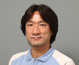
Mr. Tsuyoshi Arai
Senior Engineer, Semiconductor Production Equipment
NGL Development Div. 3
Canon Inc.
Japan
Presentatioin Title:
Nanoimprint performance Improvement for High Volume
Semiconductor Device Manufacturing
Abstract:
Nanoimprint lithography (NIL) manufacturing equipment utilizes a patterning technology that involves the field-by-field deposition and exposure of a low viscosity resist deposited by jetting technology onto the substrate. The patterned mask is lowered into the fluid which then quickly flows into the relief patterns in the mask by capillary action. Following this filling step, the resist is crosslinked under UV radiation, and then the mask is removed, leaving a patterned resist on the substrate. The technology faithfully reproduces patterns with a higher resolution and greater uniformity compared to those produced by photolithography equipment. Additionally, as this technology does not require an array of wide-diameter lenses and the expensive light sources necessary for advanced photolithography equipment, NIL equipment achieves a simpler, more compact design, allowing for multiple units to be clustered together for increased productivity.
CV:
Tsuyoshi Arai joined Canon Inc. in 2000. Involved in mechanical design of semiconductor lithography equipment. He is an engineer of flow control of air and liquid using thermal fluid simulation.
He has been engaged in the development of nanoimprint lithography equipment since 2010. He is currently leading the development of inkjet mechanisms, which are key devices in nanoimprint technology.

Dr. Stefan Finkbeiner
CEO
Bosch Sensortec GmbH
Germany
Presentation Title:
Unveiling the Future: Exploring the Transformative Power of Hearables and Wearables
Abstract:
The rise of hearables and wearables has brought about a new era of technological innovation, enabling exciting use cases that were previously unimaginable. These tiny "hearoes" are revolutionizing the way we interact with technology, offering a wide range of functionalities that enhance our daily lives.
The inclusion of a vast number of sensors in a single earbud transforms it into a miniature computer, enabling a multitude of sophisticated user interactions and use cases. This opens up a myriad of opportunities for hands-free interaction and control, simplifying access to and utilization of technology across various contexts.
Among the most compelling applications of hearables and wearables is indoor navigation. By harnessing advanced sensors and connectivity capabilities, these devices can furnish users with real-time navigation assistance in intricate indoor settings, such as shopping malls, airports, and office buildings.
This presentation delves into the technologies and devices that facilitate these use cases, culminating in an exploration of future applications and upcoming technologies, uncovering the exciting possibilities that lie ahead.
CV
Dr. Stefan Finkbeiner has been CEO and General Manager at Bosch Sensortec GmbH since 2012. He was born in 1966 in Freudenstadt, Germany.
Prior to his appointment as Bosch Sensortec’s CEO, Stefan Finkbeiner held various senior positions at Bosch including Director of Sensor Marketing, Director of Corporate Research in microsystems technology, and Vice President of Sensor Engineering. Overall, he looks back on almost 30 years in semiconductor industry working in different positions related to sensor research, development, manufacturing, and marketing.
Due to his wide experience in semiconductor and sensor industry, Stefan Finkbeiner is a recognized guest in panel discussions and as keynote speaker. Recent speaking opportunities included CES, embedded world Exhibition & Conference, SEMICON, and Global CEO summit. Additionally, he acts as member of the board of trustees of Fraunhofer ENAS and Chairman of the Governing Board of the Chips Joint Undertaking.
In 2015, Stefan Finkbeiner was awarded with the prestigious lifetime achievement award from the MEMS & Sensors Industry Group. In 2016, 2022 and 2023 he has been elected Manager of the Year by the Markt & Technik Magazine.
Stefan Finkbeiner received his diploma in physics from University of Karlsruhe (now Karlsruhe Institute of Technology) and holds a PhD in physics from Max Planck Institute and University of Stuttgart.

Dr. Takenori Fujiwara
Chief Research Associate
Toray Industries, Inc.
Japan
Presentation Title:
Advanced Packaging materials for MEMS
Abstract:
This talk covers technical trends and challenges specific to advanced packaging materials technology, especially organic cavity formation for MEMS and laser assisted transfer (mass transfer) technology for silicon photonics.
Micro-Electro-Mechanical Systems (MEMS) packaging plays a crucial role in ensuring the reliability and performance of MEMS/sensor devices. Among various packaging materials, polyimide has emerged as a prominent candidate due to its excellent thermal stability, mechanical flexibility, adhesion and chemical resistance. This paper reviews the application of polyimide in MEMS packaging, focusing on its properties, fabrication processes, and integration techniques. We discuss the advantages of polyimide over traditional materials, such as its ability to withstand high temperatures and its compatibility with various MEMS fabrication processes. Additionally, we explore recent advancements in polyimide-based packaging solutions, including its organic cavity structure, mass-transfer technology for Wafer-Level- Packaging and its role in enhancing device performance. The findings highlight the potential of polyimide to address current challenges in MEMS packaging and pave the way for future innovations in the field.
CV:
Dr. Takenori Fujiwara has more than 20 years of experience in the IT related materials. The bulk of his career has been centered on materials R&D for use in microelectronics,
photonics and display technologies, spanning a variety of senior technology.
He has spent time developing incubation technologies in consortium with A*STAR IME (Institute of Microelectronics) in Singapore since 2016. He is working on advanced packaging materials regarding FOWLP, 3DIC, Power Electronics, MEMS and Photonics applications. The materials are Polyimide, TBDB, Non-conductive film, TIM and so on.
He has published numerous advanced semiconductor material papers and holds various patents for the materials and ancillary development work. He is a team builder who combines strong business and technical acumen with excellent relationship skills.
He newly set up“Toray Singapore Research Center” at Singapore at 2022, June.
He holds a PhD in material engineering from Nagoya University.

Dr. Kaitlin Howell
Product Manager,
Marketing and Sales
Sensirion AG
Switzerland
Presentation Title:
Breaking the Cost-Size Barrier:
Next Generation Miniaturized CO2 Gas Sensors
Abstract:
Humans spend 90% of their lives indoors, driving home the importance of good indoor air quality. High CO2 concentrations in indoor environments leads to decreased cognitive performance, lower sleep quality and indicate an increased risk of viral infection. Additionally, smart regulation of ventilation through the proxy of CO2 concentration significantly improves energy efficiency. However, the cost and size of existing CO2 gas sensors has limited their penetration into the air quality market. In this presentation, Dr. Kaitlin Howell will discuss the groundbreaking work to create truly miniaturized and cost-effective CO2 gas sensors, with enormous potential to reshape how humans interact with their indoor environments. The presenter will dive into the technological leaps made to create this next generation gas sensor, then illustrate the potential applications now accessible by breaking the cost-size barrier. Finally, the implications of widespread CO2 gas monitoring in indoor environments will be discussed.
CV:
Dr. Kaitlin Howell is a product manager for the CO2 gas sensing portfolio at Sensirion. With an MSc. and PhD in Microsystems and Microelectronics from the Swiss Federal Institute of Technology (EFPL) in Lausanne, Switzerland as well as a Master of Advanced Studies in Management, Technology and Economics from the Swiss Federal Institute of Technology (ETH) in Zurich, Switzerland, she has experience in both research and strategic roles. Having transitioned from R&D to product management in 2022, her mission is to bring miniaturized sensors to market that directly impact people’s lives.
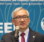
Dr. Wan-Thai Hsu
Chief Technology Officer
Soundskrit
U.S.A.
Presentation Title:
MEMS Directional Microphone – from research to products
Abstract:
A directional MEMS (Micro-Electro-Mechanical Systems) microphone is an advanced audio sensor designed to capture sound from specific directions while minimizing noise from others. This technology emulates the precise auditory capabilities found in nature, such as those of insects and spiders. The microphone's compact size and high sensitivity make it ideal for applications in modern consumer electronics, including smartphones, hearing aids, and smart devices. Its ability to discern sound direction enhances audio quality and clarity in noisy environments, providing a significant advantage for voice recognition systems and other audio applications that require high-fidelity sound capture.
This talk not only reviews the development history of directional MEMS microphones in the academics, but also provides practical insights how to make robust and reliable designs for various applications.
CV:
Dr. Wan-Thai Hsu received a Ph.D. in Electrical Engineering and an MBA from the University of Michigan. Over the past 25 years, his work in MEMS and semiconductor technologies has been recognized globally, earning him prestigious awards, such as the EE Times ACE Innovator of the Year Award (2007) and IEEE CB Sawyer Award (2015). He has held various positions of critical importance in startups as well as publicly traded companies, including CTO of Discera, CTO of MEMS at Micrel (now Microchip), CTO of TXC, CEO of Siliconquartz, and Chairman of the Board at Stathera. He is a senior member of IEEE, chaired the annual IEEE Frequency Control Symposium in 2014 and co-chaired the decennial IEEE UFFC Joint Symposium in 2024.
Currently, Dr. Hsu is the Chief Technology Officer at Soundskrit, which aims to develop bio-inspired MEMS audio systems to provide the capability not only to capture sound with high quality, but also to distinguish sound localization. He leads the overall product development, manufacturing, packaging, and production testing to actualize high performance MEMS directional microphones. Soundskrit therefore was named the top 100 startups to watch by EE Times in 2023 and 2024.

Dr. Cheng-Hao (Kevin) Ko
Associate Professor,
Graduate Institute of Automation and Control
National Taiwan University of Science and Technology
Taiwan
Presentation Title:
SPU X GPU to Enable Health Future
Abstract:
SPU x GPU
We are reshaping the future of human healthcare monitoring from individual to global scale.
SPU (Spectrum Processing Unit) technology enables instant, constant, accurate, self-operable, low cost, multiple-item and decentralized healthcare monitoring.
SPU technology is based on spectral detection principle, which is the most commonly used and most accurate quantification method worldwide. Endless test items can be added to the list using one single SPU device.
With the integration of SPU and GPU, we are able to construct an AI doctor to provide disease-prevention suggestions and health risk-factor assessment based on personal health big data generated by the SPU-POCT (Point of Care Testing) device.
CV:
Dr. Ko Cheng-Hao has been engaged in the design, construction, and integration of high-efficiency micro-optical systems for 23 years, collaborating with various academic and research institutions. His superior technology and exceptional capabilities have led to his recruitment by key research units to lead technology development and assist in the growth of innovative industries. From 1990 to 1995, he participated in the design and construction of the grating spectrometer system for the Beamline X1A at the National Synchrotron Light Source, Brookhaven National Laboratory, USA, with a construction budget of NT$500 million. He is the inventor and designer of the world's first synchrotron X-ray photoelectron high-resolution microscopy instrument. From 1995 to 2000, he led the construction project of the U5 beamline experimental station at the National Synchrotron Radiation Research Center (NSRRC) in Taiwan, with a construction budget of NT$300 million, successfully developing X-ray photoelectron high-resolution microscopy technology for the Taiwan Synchrotron Radiation Center (U5-SpectroMicroscopy End Station at NSRRC, ROC), and participated in the design and construction of the beamline grating spectrometer system.
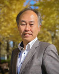
Dr. Hiroyuki Kuchiji
Advanced Specialized Manager, Element Device Development Department,
New Business Development Division
Nisshinbo Micro Devices Inc.
Japan
Presentation Title:
Transition of Nisshinbo Micro Devices' MEMS microphone business and
cutting-edge MEMS microphones
Abstract:
Nisshinbo Micro Devices is an electronic device manufacturer of the Nisshinbo Group that was established in 2022 through the merger of New Japan Radio Co., Ltd. and RICOH Electronic Devices Co., Ltd. Through electronic devices and microwave products that have analog technology as their strength, we aim to contribute to the development of a connected society and become a company with value and presence that is expected by customers around the world.
Our MEMS business began developing MEMS microphones in 2006 and began mass production in 2011. With the subsequent expansion of the mobile device market, we have shipped a cumulative 3 billion MEMS transducers to date. Currently, we are working on the development of various MEMS sensor devices in addition to microphones. Furthermore, going forward, we will not be limited to the sensor device business alone, but will utilize AI and other software technologies to provide high-value solutions to the challenges facing society and our customers.
In our presentation, we will focus on the history of the MEMS microphone business and provide the latest information on piezoelectric MEMS microphones using ScAlN and capacitive MEMS microphones using metallic glass.
CV:
Dr. Hiroyuki Kuchiji joined New Japan Radio Co., Ltd., the predecessor of Nisshinbo Micro Devices Inc., in 1995 and has over 20 years of experience in integrated circuit process and device development. He is an expert in metallization of integrated circuits and optoelectronic integrated circuits, has launched several CMOS and Bi-CMOS processes, and has been involved in the development of numerous IC products. Since 2016, he has been working on research and application development of piezoelectric MEMS. He has obtained approximately 30 patents related to sensors and their applications. He was a visiting professor at Kyushu Institute of Technology from 2019 to 2021, where he provided consulting on CMOS processes. He received his Ph.D. degree from Kyushu Institute of Technology in 2024. Recently, he has been working with group companies to develop medical devices and predictive maintenance systems.
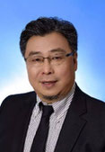
Prof. Xinxin Li
Director, State Key Lab of Transducer Technology
Shanghai Institute of Microsystem and Information Technology, Chinese Academy of Sciences
China
Presentation Title:
MIS process---A versatile MEMS batch fabrication technology for transducers
Abstract:
A novel MIS (micro-holes inter-etch & sealing) process is addressed that features single-wafer single-sided fabrication of complicated 3D MEMS structures with very high yield and ultra-low cost. The process is suitable for batch fabrication of micro sensors in standard semiconductor foundries. A start-up company of Shanghai MIS technology Co. Ltd. has been created to produce pressure sensors, gas sensors, flowmeters and infrared detectors with the MIS processing technology and the process has been implemented in 6 and 8-inch MEMS R&BD foundries to volume produce the sensor chips. The sensors manufactured with the MIS process and its updated versions of TUB (thin-film under bulk-Si) and BUT (bulk-Si under thin-film) are advantageous in tiny size, high performance and high performance uniformity, thereby have been widely used in various applications.
CV:
Prof. Xinxin Li received B.S. degree from Tsinghua University and Ph.D. degree from Fudan University. He was engaged as Research Associate in Hong Kong University of Science and Technology, Research Fellow in Nanyang Technological University, Singapore, and COE-Fellow Researcher in Tohoku University, Japan. Since 2001, he has been a Professor of Shanghai Institute of Microsystem and Information Technology, Chinses Academy of Sciences, where he had served as the director of State Key Lab of Transducer Technology of China. He is also an Adjunct Professor for Fudan University and ShanghaiTech University.
His research interest includes micro/nano sensing and detection technology, MEMS/NEMS technology and analytical-chemistry instrumentation technology. He was granted the National Science Fund of China for Distinguished Young Scholar in 2007. His Ph.D. student was awarded National Excellent 100 Ph.D. Dissertation in 2009. He has invented more than 200 patents and published more than 600 articles in refereed journals and conferences (including more than 300 SCI journal articles) with total citation of more than 10 thousands. He served as TPC member for IEEE MEMS and IEEE Sensors. Now he serves the conference of Transducers as the Asia/Oceania regional TPC Chair. He is Associate Editor and Editorial Member for Microsystema and Nanoengineering, J Micromech. Microeng., Scientific Reports, and, Micromachines.
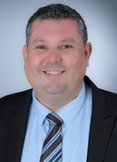
Mr. Jérome MOULY
Director - Sensing, Imaging and Display
YOLE GROUP
France
Presentation Title:
Dynamics and trends of the MEMS and PiezoMEMS market
Abstract:
The MEMS industry, expected to reach $20B in 2029, is at a critical point, navigating both challenges and growth. Despite setbacks in 2023 and 2024, the sector continues to benefit from key megatrends like autonomous driving, AI, and Industry 4.0, driving demand forward. In the MEMS industry, Piezo-MEMS technology is standing out as a significant growth area. This technology improves performance and introduces new functionalities, enabling innovations like MEMS microspeakers, PMUT, or MEMS laser beam scanning. Piezo-MEMS relies on thin-film deposition of piezoelectric materials (such as PZT or AlN), chosen based on the device’s application. To overcome technical challenges, a strong ecosystem of specialized equipment providers and foundries has emerged. This presentation will explore future opportunities and the evolving dynamics within the PiezoMEMS landscape.
CV:
Jérôme Mouly is Director of Sensing, Imaging and Display activities at Yole Group.
Jérôme manages the expansion of the technical expertise and market know-how of the team. In addition, Jerome’s mission focusses on the management of business relationships with company leaders and the development of market research and strategy consulting activities.
He has conducted more than 100 marketing and technological analyses for industrial groups, start-ups, and institutes in the field of MEMS and sensing technologies.
Jérôme has been also deeply engaged in Yole Group's finance activities with a dedicated focus on the commercial exploitation of smart system technologies and access to funding opportunities.
Jérôme is regularly involved in international conferences, with presentations and keynotes.
Jérôme Mouly earned a Master of Physics degree from the University of Lyon (FR).

Dr. Kurt Petersen
Silicon Valley Band of Angels
U.S.A.
Presentation Title:
My 50 Years in MEMS
Abstract:
After receiving my PhD from MIT in 1975, I interviewed for jobs at TI, IBM, and Xerox PARC. While visiting PARC in Palo Alto, the Xerox folks gave me a tour of the Stanford labs of Professor Jim Angel. I was stunned to see academic posters for an accelerometer and a gas chromatograph fabricated on silicon wafers. I eventually joined IBM Research in San Jose, not far from Stanford. While touring around the research Building 28 at IBM, I noticed a huge black stain on the tile hallway outside of one laboratory. I was stunned again to see that the occupants were developing tiny ink jet nozzle arrays by etching minute holes in silicon wafers – the test set-up had leaked. MORE mechanical devices on silicon? I was hooked! Within a short time, I put together my own research program at IBM to build mechanical devices on silicon, published a number of papers, and wrote the review paper “Silicon as a Mechanical Material” in 1982. Since leaving IBM in 1982, I have been involved in developing commercial MEMS-based products in six start-up companies, 2 of which went IPO (Cepheid and SiTime) and 2 of which were acquired (Verreon by Qualcomm and NovaSensor by Amphenol). This talk will discuss the ups and downs of MEMS product development and the significant MEMS product and process milestones over the past 50 years.
CV:
Kurt Petersen received his BS degree cum laude in EE from UC Berkeley in 1970, and a PhD in EE from the Massachusetts Institute of Technology in 1975. Since 1982, he has co-founded six successful, high-tech companies in Silicon Valley, including NovaSensor (now owned by Amphenol), Cepheid (acquired by Danaher in 2016 for $4B), and SiTime (SITM on NASDAQ). In 2001, he was awarded the IEEE Simon Ramo Medal for his contributions to MEMS. Dr. Petersen is a member of the National Academy of Engineering and is a Life Fellow of the IEEE in recognition of his contributions to “the commercialization of MEMS technology”. In 2011, Dr. Petersen joined the Silicon Valley Band of Angels. Today, he spends most of his time helping and mentoring early stage, high-tech start-up companies. In 2019, Dr. Petersen was awarded the IEEE Medal of Honor, IEEE’s highest tribute.

Mr. Paul Pickering
Managing Partner
Silicon Catalyst
U.S.A.
Presentation Title:
MEMS Role in Emerging Infrared Sensing and Imaging Applications
Abstract:
The MEMS industry has played a significant role in the development of various thermal sensing technologies. MEMS-based Bolometers have addressed the high end of the thermal imaging market, but the cost and trade restrictions have often limited the number of applications that can be addressed. Many new approaches to thermal sensing and image detection have been proposed in recent years. MEMS technologies are enabling engineering to develop various new structures for applications like high-resolution image detection, low-cost spectrometers, zero-power switch mechanisms, gas sensors, and presence detection for smart cities. In my presentation, I will discuss the variety of applications and the role MEMS will play as these solutions ramp into high volume.
CV:
Paul Pickering has been a passionate advocate for emerging semiconductor and sensor technologies during the length of his 40-year career. He has worked with an extensive array of technologies and has also been on the founding team of two semiconductor start-ups. Paul is an active investor in the area of early-stage, deep-tech technologies. He is the Managing Director of Microtech Ventures and Managing Partner at Silicon Catalyst. Both organizations have numerous angel investments. He recently accepted a Board of Directors role at Silicon Catalyst Angels. During his corporate career, he was an executive at two public companies that have subsequently been acquired. From 2015 to 2019, he was the Chief Revenue Officer for Micralyne Inc., based in Edmonton, Alberta, Canada. In August 2019, Micralyne was acquired by Teledyne Technologies.
Paul graduated from West Chester University of Pennsylvania with a Bachelor of Science degree and also attended Widener University in Chester, Pennsylvania. He is a recognized speaker at technology conferences and trade events in the semiconductor and MEMS industries.

Dr. Arne Quellmalz
CEO
In2great Materials
Sweden
Presentation Title:
Wafer-level integration of 2D materials for back-end of line applications
Abstract:
Layered materials with thicknesses on the atomic scale (2D materials) promise to revolutionize electronics and photonics. Yet, the realization of this potential is hindered by the lack of a viable integration technology that can seamlessly leverage the well-established silicon-based semiconductor manufacturing infrastructure at an industrial scale. Without such a solution, the transformative capabilities of 2D materials may never extend beyond academic research, failing to unlock their full potential in practical applications.
In this talk, we showcase advancements in the integration of 2D materials through an innovative wafer-scale transfer technique developed by the start-up company In2great Materials AB. Our solution is based on adhesive wafer bonding and utilizes equipment, processes, and materials readily available in large-scale semiconductor manufacturing lines. Offering compatibility with fully automated tools and independence from recipient wafer topography and surface properties, our approach facilitates the integration of large area 2D materials onto most processed device substrates. These advantages effectively lower the barriers for industry adoption.
CV:
Arne Quellmalz is the co-founder and chief executive officer (CEO) of the Swedish start-up company In2great Materials AB. In2great Materials enables the development of future electronics by offering the semiconductor industry solutions for integrating atomically thin materials. Arne earned a Ph.D. in Electrical Engineering from the KTH Royal Institute of Technology (Sweden) with a research focus on photonic microsystems and 2D material integration.

Dr. Florian Schuster
Product Management
MEMS Sensors
Robert Bosch GmbH
Presentation Title:
Exploring New Frontiers with Bosch: High-Bandwidth and precise Low-G Sensors for innovative applications in the automotive market
Abstract:
MEMS sensors have long since become integral to many applications in the consumer and automotive domain. Yet Bosch continuously innovates to meet new emerging demands within these highly mature markets. This presentation will provide an overview of Bosch's latest low-g MEMS sensors and their applications.
Key topics include:
- the role of high-bandwidth low-g accelerometers in Road Noise Cancellation (RNC) and predictive maintenance,
- the use of precise low-g sensors for headlight-leveling,
- and the detection of vehicle inclination to identify malfunctions and vandalism in radar and ultrasonic systems.
Attendees will gain insights into the specific needs of these new applications and how Bosch's cutting-edge low-g sensors address them effectively.
CV:
Dr. Florian Schuster is a physicist by education and has been working at Bosch for the past 16 years in the area of automotive MEMS sensors in a variety of roles. Since November 2025 he is responsible for the product management and the development of new business fields for the automotive MEMS business unit at Bosch.

Mr. Naoaki Shirakawa
Senior Manager, Product marketing section,
Thin film device department, Passive device division,
Component business unit
Murata Manufacturing Co., Ltd.
Japan
Presentation Title:
Latest Trend of Silicon Capacitor
Abstract:
Since Murata started the silicon capacitor business in 2016, its demand has been increasing. It is because feature of silicon capacitor contributes to solving new challenges in cutting-edge applications such as xPU for smartphone and AI/HPC server, optical communication, etc. In my presentation, I will introduce basic information on its feature such as very thin down to 50um with high capacitance and low ESL simultaneously, after that background of the demand in each application.
CV:
2008 : Joined Murata Manufacturing Co., Ltd. and responsible for technical marketing & promotion for the general MLCC business.
2009 : Responsible for technical marketing & promotion for the EMI products in addition to general MLCC.
2011 : Responsible for technical marketing & promotion for application-specific MLCC.
2016 : Responsible for technical marketing & promotion for silicon capacitor.
2017 : Manager of technical marketing & promotion for silicon capacitor.
2019 : Manager of business planning for silicon capacitor.
2023 : Senior manager of technical marketing & promotion for silicon capacitor.

Mr. Collin Twanow
Director of Technology
Teledyne MEMS
Canada
Presentation Title:
Evolution of a MEMS Foundry for the Future
Abstract:
MEMS manufacturing has always encountered unique challenges and opportunities. This talk will touch on the history and evolution of two fabs that have become the Teledyne MEMS foundry business. The presenter will introduce our view of new MEMS and microfabrication opportunities that use wafer level stacking of CMOS, MEMS, and packaging wafers to achieve a higher level of integration and cost reduction. Special attention will be given to the fabrication equipment needed for this evolution. Emerging technologies such as silicon photonics and biomedical analysis on chip will be discussed to ensure a rich development roadmap for MEMS foundries.
CV:
Collin has worked in MEMS and microfabrication for more than 25 years and is currently the Director of Technology for Teledyne MEMS. Previously he held various roles in Engineering Management and Sales. He is primarily responsible for managing strategic accounts and collaborating with customers and internal stakeholder’s technology development and expansion. Collin is also responsible for technical problem solving and communicating Teledyne MEMS capabilities to the MEMS market.
Collin has managed development programs for many devices including optical telecom switches, silicon optical bench, implantable medical devices, MEMS microphones, pressure sensors, accelerometers, and components for military applications.
Collin is a Professional Engineer and holds a B.Sc in Engineering Physics as well as a Master’s of Electrical Engineering degree with a specialization in Microfabrication Collin has also lectured on microfabrication topics at the University of Alberta.
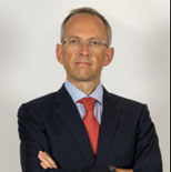
Mr. Beneditto Vigna
Chief Executive Officer
Ferrari
Presentation Title:
Emotions wins over technology
CV:
Benedetto Vigna is Chief Executive Officer since September 2021.
Before joining Ferrari, he was President of STMicroelectronics’, Analog, MEMS and Sensors Group, since January 2016 and also a member of ST’s Executive Committee from May 31, 2018. Vigna joined ST in 1995 and founded the Company’s MEMS activities (Micro-Electro-Mechanical Systems). Under his guidance, ST’s MEMS sensors established the Company’s leadership with large OEMs in motion-activated user interfaces. His responsibilities were expanded to include connectivity, imaging and power solutions and he piloted a series of successful moves into new business areas, with a particular focus on the industrial and automotive market segments. During his career Vigna has filed more than 200 patents on micromachining, authored numerous publications and has sat on the Boards of several EU-funded programs including start ups as well as worldwide recognized Boards of Asian and American research centers. Benedetto Vigna graduated in Subnuclear Physics from the University of Pisa.
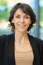
Professor Dana Weinstein
Professor, Elmore School of Electrical and Computer Engineering
Purdue University, U.S.A.
Presentation Title:
MEMS for CHIPS and CHIPS for MEMS
Abstract:
Between industry, academia, national labs, governments, and global partnerships, the whole of the chips community recognizes the need and urgency in joining forces to bolster both manufacturing and innovation in microelectronics. MEMS offer unique capabilities, know-how, and infrastructure to support the needed advancements in microelectronics. Similarly, the broad investments and recognition of rapid need to adapt, innovate, and diversify technology platforms opens up new opportunities for MEMS. How can we best leverage this momentum? What are some of the biggest opportunities and challenges ahead for academia, for regional ecosystems, and for emerging tools like AI to accelerate innovation to address global challenges on timescales needed for real impact?
CV:
Dana Weinstein is a Professor in Purdue’s Elmore Family School of Electrical and Computer Engineering. Prior to joining Purdue in 2015, Dr. Weinstein was a Professor at MIT in the Department of Electrical Engineering and Computer Science. She received her B.A. in Physics and Astrophysics from UC Berkeley in 2004 and her Ph.D. in Applied Physics in 2009 from Cornell. She is a Purdue Faculty Scholar, and a recipient of IEEE UFFC Sawyer Award, the NSF CAREER Award, the DARPA Young Faculty Award, the first Intel Early Career Award, the first TRF Transducers Early Career Award, and the IEEE IEDM Haken Award. Dr. Weinstein’s research focuses on innovative microelectromechanical devices for applications ranging from MEMS-IC wireless communications and clocking to harsh environment sensors and ultrasonic stimulation. Professor Weinstein has served as Associate Director for Purdue's Birck Nanotechnology Center, as Associate Dean in the College of Engineering at Purdue, and most recently as Principal Assistant Director and Special Advisor for Microelectronics Research and Development at the White House Office of Science and Technology Policy in DC. In that role, she is also a champion for accelerating materials innovation through autonomous experimentation.
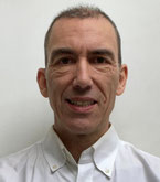
Mr Mark Wood
VP
xMEMS GK
Japan
Presentation Title:
The X Factor in MEMS Innovation: Breakthroughs Across Three Product Lines With a Single Platform
Abstract:
xMEMS has developed a MEMS platform which currently supports three product lines, including microspeaker, dynamic vent and microcooler. Utilizing a monolithic piezoMEMS process for all products has resulted in exceptional production uniformity and consistency, robustness, dust and moisture resistance, low power and small size. The recently announced xMEMS micro cooler product is the world’s thinnest fan at only 1mm thick.
CV:
Mark Wood is the Vice President of xMEMS GK, responsible for sales and technical support of customers in Japan. He has worked in the electronics industry in Japan for over 35 years and the MEMS industry for over 15 years. Previous roles include analog and digital electronic circuit design engineering, customer technical support management, including MEMS gyroscope, accelerometer, pressure, microphone, time-of-flight and fingerprint sensor products. He holds a Masters Eng MicroElectronics from Middlesex University London UK.

Dr. Yu Yanagisawa
Representative Director, CEO
CellFiber Co., Ltd.
Japan
Presentation Title:
The Ongoing Journey of CellFiber Technology from Lab to Industry
Abstract:
CellFiber is a Tokyo-based startup established in 2015, rooted in proprietorial technology developed at the Institute of Industrial Science of the University of Tokyo. Our mission is to make this innovative technology accessible beyond academic circles, driving its widespread adoption of the transformative potential of 3D cell culture to revolutionise the way therapeutic cells are produced.
In 2020, significant strides were made by applying our technology in cultures of a diverse cell types. Building upon these accomplishments, in 2023, we directed our effort towards developing products and processes that comply with industrial standards and regulatory guidelines, ensuring our commitment to excellence and innovation to improve patient outcomes and medical advancements remains unwavering. In this presentation, I will share the journey we undertook to release our lab-born technology as an industrial application, detailing the challenges we encountered along the way and how we overcame them.
CV:
2018 – Present, CellFiber Co., Ltd.
Joined CellFiber in 2018 and was appointed as CEO within one year. Leading the company’s strategic initiatives, including raising a total of 2.5 billion yen in funding, driving global talent acquisition, and overseeing product and process development.
2011 – 2017, Ph.D student, Graduate School of Engineering, The University of Tokyo
Conducted research in soft material sciences, specializing in functional materials utilizing bent hydrogen bonds. Published research findings in peer-reviewed journals, including Science, contributing to advancements in the field of soft materials.
2007 – 2011, Leave a Nest Co., Ltd.
Worked on interdisciplinary research projects, applying scientific expertise to bridge academic and industrial applications.

Dr. Kara Zappitelli
Foundry Director
Science Corporation
U.S.A.
Presentation Title:
The Role of MEMS in the Burgeoning Brain Computer Interface Industry
Abstract:
The Brain Computer Interface (BCI) industry is growing at record pace, with an estimated TAM of $400B in the US alone and plenty of room to grow. However, many barriers to commercialization and adoption still exist, one of which is the availability of low-cost, scalable manufacturing with clinical-grade quality. Next generation medical devices require unique consideration of materials, packaging, hermiticity, etc, not often found in standard MEMS foundries, forcing BCI companies to establish expensive internal manufacturing capabilities, thereby extending timelines and reducing runway. In addition, high costs of prototyping further discourage innovation at all technology readiness levels. Science Foundry leverages established MEMS foundry infrastructure and our own internal medical device manufacturing expertise to enable companies at the forefront of technology. Through custom process development, post-CMOS processing, or off-the-shelf neural probe offerings, we aim to accelerate commercialization timelines and lower barriers to widespread adoption of BCI technologies.
CV:
Dr. Kara Zappitelli received her Ph.D. in Physics from the University of Oregon in 2020 and has more than a decade of experience in microfabrication for MEMS and medical devices. She joined Science Corporation as employee number seven in 2021, where she designed and fabricated the first five prototypes of the company’s wafer-scale optogenetic, flexible retinal prosthesis. In December of 2022, Science Corporation acquired a North Carolina based MEMS Foundry from MEMSCAP as part of their efforts to vertically integrate medical device production and Kara relocated to Research Triangle Park to lead technical efforts at Science Foundry, build the team, and drive process translation of the company’s retinal implants and other devices. In her current role as Foundry Director, Kara has worked to re-build, re-tool, and re-vamp the fab. She leads an efficient team of engineers and technicians, and her efforts have more than doubled wafer throughput. Kara’s expert management has seen Science Foundry emerge as a leading US-based fab that partners with researchers and companies around the world on the production of high-quality MEMS devices. In 2024, she was recognized by SEMI as an Emerging Leader.

 MEMS Engineer Forum (MEF) 2025
April 16-17, 2025
KFC Hall, Ryogoku, Tokyo, Japan


