Tuesday, April 21, 2026
| Time | Presentation Title | Speaker |
|---|---|---|
| 9:00 – 9:10 | Opening Remarks | Prof. Shuji Tanaka Tohoku University/MEF Organizing Committee Chair |
Session 1: Now & Future of MEMS Chairperson: Prof. Taeko Ando, Ritsumeikan University/MEF Organizing Committee Vice Chair |
||
| 9:10 – 9:50 | Keynote Speech Smart Materials, Smarter Devices: Piezoelectric Thin Films in MEMS Applications | Prof. Weiliun Fang NTHU Chair Professor, Power Mech. Eng. Department,National Tsing Hua University,Taiwan |
| 9:50 – 10:15 | Invited Speech MEMS market regains momentum: trends and strategic consolidations | Mr. Jerome Mouly Director – Imaging and Sensing activities, YOLE GROUP, France |
| 10:15 – 10:40 | Invited Speech Next-generation MEMS, applications and technologies | Mr. Mika Takahashi Senior Technology Analyst, IDTechEx K.K, U.K. |
| 10:40 – 10:50 | Break | |
Exhibitor Presentation Session 1 Chairpersons: Koichi Ohtaka, Tohoku University/MEF Organizing Committee & Hiroyuki Kuchiji, Nisshinbo Micro Devices/MEF Organizing Committee |
||
| 10:50 – 12:20 | Exhibitor Presentation | |
| 12:20 – 13:50 | Lunch & Exhibit Hour | |
Session 2: R&D, manufacturing and applications Chairperson: Yoshiaki Oku, Rohm/MEF Organizing Committee |
||
| 13:50 – 14:15 | Invited Speech MEMS no Shinpo: Advancing the Future with Illustrative Applications in Microphone MEMS and Optomechanical Sensing | Dr. Pierre-Damien Berger MEMS Industrial Partnerships Manager, CEA LETI, France |
| 14:15 – 14:40 | Invited Speech Fast-Tracking PiezoMEMS: From Concept to Manufacturing Readiness | Dr. Yao Zhu Head of Department / MEMS, Institute of Microelectronics, A*STAR, Singapore |
| 14:40 – 15:05 | Invited Speech Beyond the Hype: Quantum Sensors for Practical Applications | Dr. Tino Fuchs Senior Expert for Quantum Sensors, Robert Bosch GmbH, Germany |
Exhibitor Presentation Session 2 Chairperson: Masaki Hirose, Hamamatsu Photonics K.K./MEF Organizing Committee |
||
| 15:05 – 15:50 | Exhibitor Presentation | |
| 15:50 – 16:30 | Exhibit Hour | |
Session 3: ICEP Special Session Chairperson: Hiroshi Miyajima, SUMITOMO PRECISION PRODUCTS, Co., Ltd./MEF Organizing Committee |
||
| 16:30 – 17:10 | Keynote Speech The Made-in-Japan Challenge: A Paradigm Shift Enabled by Chiplet Technology | Dr. Yasumitsu Orii Senior Managing Executive Officer, Head of Engineering Center, Rapidus Corporation, Japan |
| 17:10 – 17:35 | Invited Speech Advancements in Direct Transfer Bonding (DTB) for High-Precision Integration of Ultra-Thin and Delicate Chips | Mr. Ichiro Sano Chief DTB Researcher/Development Dept., Tazmo co.,LTD, Japan |
| 17:35 – 18:05 | Break/Lottery | |
| 18:05 – 19:35 | Networking Reception | |
Wednesday, April 22, 2026
| Time | Presentation Title | Speaker |
|---|---|---|
| 8:30 – 8:35 | Opening Remarks | Prof. Shuji Tanaka Tohoku University/MEF Organizing Committee Chair |
Session 4: Foundry and Fabless Chairperson: Jun Iida, TDK Corporation/MEF Organizing Committee |
||
| 8:35 – 9:15 | Keynote Speech The Next Decade of MEMS Manufacturing and Technology– A View from The World’s Largest Pure-Play MEMS Foundry | Dr. Niklas Svedin CTO, Silex Microsystems AB, Sweden |
| 9:15 – 9:40 | Invited Speech Advancements in Silicon Photonics and MEMS Through Heterogeneous Integration | Dr. Stefan Ernst Director Business & Strategy, X-FAB MEMS Foundry, Germany |
| 9:40 – 10:05 | Invited Speech Syntiant: Making Edge AI a reality with MEMS Sensors | Mr. Hiroshi Suzuki Representative Director, Syntiant Japan KK, Japan |
| 10:05 – 10:30 | Invited Speech AirJetTM – A Novel Heat Dissipation Device | Dr. Suryaprakash Ganti Founder/CTO, Frore Systems, USA |
| 10:30 – 10:40 | Break | |
Exhibitor Presentation Session 3 Chairperson: Hiroyuki Wado, MIRISE Technologies/MEF Organizing Committee |
||
| 10:40 – 11:45 | Exhibitor Presentation | |
Panel Discussion |
||
| 11:45 – 12:35 | Theme: Learning from failure in MEMS | Panelists: Prof. Weileun Fang,NTHU Chair Professor, Power Mech. Eng. Department, National Tsing Hua University, Taiwan Dr. Kurt Petersen, Silicon Valley Band of Angels, USA Dr. Pierre-Damien Berger, MEMS Industrial Partnerships Manager, CEA LETI, France Dr. Suryaprakash Ganti, Founder/CTO, Frore Systems, USA Moderator: Dr. Hiroshi Miyajima, Sumitomo Precision Products/Chair of MEF Program WG, Japan |
| 12:35 – 14:05 | Lunch and Exhibit Hour | |
Session 5: Frequency/Resonance and Drug Discovery Chairperson: Akihiro Koga, Canon Medical Systems Corporation/MEF Organizing Committee |
||
| 14:05 – 14:30 | Invited Speech SiTime MEMS: Vision and Persistence that Redefined Timing | Dr. Paul Hagelin Vice President, MEMS Engineering, SiTime Corporation, USA |
| 14:30 – 14:55 | Invited Speech XBAR Technology for RF Filter Applications | Dr. Patrick Turner CTO, Resonant Inc., a Murata Company, USA |
| 14:55 – 15:20 | Invited Speech Silicon Resonant Sensor Technology: Applications in Tsunami Disaster Mitigation | Mr. Shuhei Yoshita Yokogawa Products Headquarter Sensing Center, Yokogawa Electric Corporation, Japan |
| 15:20 – 15:45 | Invited Speech Drug Discovery Innovation and Social Implementation Enabled by Microphysiological Systems (MPS): Opportunities from Japan | Prof. Ryuji Yokokawa, Professor, Kyoto University/CTO, Physios Biotech, Inc., Japan Dr. Ichiro Miki, CEO, Physios Biotech, Inc., Japan |
| 15:45 – 16:15 | Exhibit Hour | |
Session 6: Integreation and Equipment Chairperson: Keiichi Umeda, Murata Manufacturing Co., Ltd./MEF Organizing Committee |
||
| 16:15 – 16:40 | Invited Speech Smart Surfaces Through IMSE® Integration | Dr. Pälvi Apilo Chief Technology Officer (CTO), TactoTek, Finland |
| 16:40 – 17:05 | Invited Speech MBM™ series: MEMS-Enabled Electron Multi-Beam Mask Writer for EUV Lithography | Mr. Kazuyuki Higashi Chief Specialist, Micro Electronics Development Group, Mask Lithography Development Department, NuFlare Technology, Japan |
| 17:05 – 17:30 | Invited Speech Advances in thin films enabled by Lam Research’ Pulsed Laser Deposition platform for MEMS applications | Dr. Matthijn Dekkers Director Engineering, Lam Research, The Netherlands |
| 17:30 – 17:55 | Invited Speech Enabling the Future of RF Filters: High-Performance Thin Films for BAW Technology | Dr. Oguz Yildirim Product marketing Manager, Evatec AG, Switzerland |
| 17:55 – 18:00 | Closing Remarks | Prof. Taeko Ando, Ritsumeikan University/MEF Organizing Committee Vice Chair |
Speakers of MEF 2026
Tuesday, April 21, 2026
9:10 – 9:50 Keynote Speech
NTHU Chair Professor, Power Mech. Eng. Department, National Tsing Hua University
Taiwan
Smart Materials, Smarter Devices: Piezoelectric Thin Films in MEMS Applications
Abstract:
Piezoelectric materials are regarded as smart materials and have been widely applied in various fields such as ultrasound probes, precision positioning systems, sonar, vibration sensors, buzzers, and so on. In recent years, with the advancement of fabrication technologies, piezoelectric thin films have become one of the key technologies driving the development of micro sensors and actuators. This talk will begin with a brief introduction to the properties of piezoelectric thin films. It will then highlight several representative application cases to showcase the potential and achievements of piezoelectric thin films in advanced MEMS devices, including micro-optical systems such as the LiDAR, and head-up displays; and the micro-acoustic systems such as the speakers. It is hoped that the sharing in this talk will inspire new opportunities for advancing piezoelectric thin film technologies and applications.
CV:
Prof. Fang has been working in the MEMS field for more than 20 years. He received his Ph.D. degree from Carnegie Mellon University (Pittsburgh, PA) in 1995. He joined the National Tsing Hua University (Taiwan) in 1996, where he is now a Chair Professor. He became the IEEE Fellow in 2015 to recognize his contribution in MEMS area. Prof. Fang has published ~500 refereed papers and granted ~120 patents. He is now the Chief Editor of JMM, the Board Member of IEEE TDMR and Sensors and Materials, and the Associate Editor of IEEE Sensors J. He served as the General Chair or Program Chair for many important international conferences: the World Micromachine Summit 2012, IEEE Sensors 2012, and Transducers 2017. He also served as the chair of International Steering Committee of Transducers during 2017-2019. Moreover, he served as the Technical Program committee of IEEE MEMS and Transducers for many years. So far more than 60 PhD and 120 Master students have graduated from Prof. Fang’s group. Most of them are working in the MEMS and micro sensors related companies. Thus, Prof. Fang has close relation with MEMS industries, and is now the Vice Chair of MEMS and Sensors Committee of SEMI Taiwan.
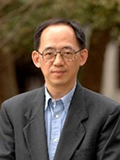
9:50 – 10:15 Invited Speech
Director – Imaging and Sensing activities, YOLE GROUP
France
MEMS market regains momentum: trends and strategic consolidations
Abstract:
2024 brought renewed momentum to the MEMS industry, with global revenues estimated at $15.4B (+5% YoY) and growth projected at a 3.7% CAGR over 2024–2030. This momentum is still on its way in 2025. As the industry continues to mature, MEMS players are strengthening and consolidating their expertise to better address key trends and challenges related to product development, volume scalability, and profitability across automotive, consumer, AI, and robotics markets. At the same time, the global MEMS industry is entering a new phase of consolidation, driven by rising technology complexity, increasing capital intensity, and the need for clear strategic positioning. This presentation will provide an update of the MEMS market and its latest trends, as well as insights into evolving ecosystem dynamics and structural changes.
CV:
Jérôme Mouly is Director of Sensing & Imaging Activities at Yole Group.
Jérôme manages the expansion of the technical expertise and market know-how of the team. In addition, Jerome’s mission focusses on the management of business relationships with company leaders and the development of market research and strategy consulting activities.
He has conducted more than 100 marketing and technological analyses for industrial groups, start-ups, and institutes in the field of MEMS and sensing technologies.
Jérôme has been also deeply engaged in Yole Group’s finance activities with a dedicated focus on the commercial exploitation of smart system technologies and access to funding opportunities.
Jérôme is regularly involved in international conferences, with presentations and keynotes.
Jérôme Mouly earned a Master of Physics degree from the University of Lyon (FR).

10:15 – 10:40 Invited Speech
Senior Technology Analyst, IDTechEx K.K
U.K.
Next-generation MEMS, applications and technologies
Abstract:
What will the next breakthrough of MEMS look like? As the MEMS market continues to evolve, new technologies continue to unlock applications for the industry. This presentation by IDTechEx will focus on two key emerging next-gen MEMS technologies, high-performance gyroscopes and micro-speakers. This presentation will aim to cover the market drivers for these products, the technical barriers to achieving high-performance microsensors and micro-speakers and what innovations are on the roadmap to commercialization. IDTechEx will cover the key players in each of these fields, from incumbent industry giants to disruptive startups. It will also provide an overview of IDTechEx’s outlook for the next decade of advanced MEMS technologies.
CV:
Mika Takahashi is a Senior Technology Analyst at IDTechEx, focusing Electric Vehicles, advanced materials, sensors, and telecoms technologies. Prior to joining IDTechEx in 2023, Mika graduated with First Class Honors from the University of Edinburgh with an MPhys (Master’s in Physics). During his final year he conducted research on novel methods of locomotion in granular systems, with commercial applications in the agriculture industryHe is currently based in Glasgow, UK.
With IDTechEx, Mika’s research has covered EVs, hydrogen internal combustion engines, MEMS, and various applications of emerging advanced materials. He has also presented at several major global events, and continues to actively travel and carry out research.

13:50 – 14:15 Invited Speech
MEMS Industrial Partnerships Manager, CEA LETI
France
MEMS no Shinpo: Advancing the Future with Illustrative Applications in Microphone MEMS and Optomechanical Sensing
Abstract:
The field of Microelectromechanical Systems (MEMS) has evolved significantly since the 1980s, transitioning from simple capacitive sensors to highly sensitive piezoresistive sensors. This presentation will outline the development roadmap for MEMS, emphasizing innovative materials and sensing technologies that are driving next-generation devices, particularly in microphone MEMS and optomechanical sensing.
Microphone MEMS: Advances in microphone MEMS include air-to-vacuum transducing mechanisms and vacuum cavities, which enhance signal-to-noise ratio (SNR) and robustness. These improvements enable MEMS microphones to excel in various applications, from medical to automotive.
Optomechanical Sensing: Optomechanical sensing uses light for motion detection, offering extreme sensitivity (femtometer detection), ultra-rapid response in the terahertz range, and superior integrability with 200 nm VLSI MEMS and photonic integrated circuit technologies. This technology has numerous applications, including:
• Portable in-situ mass spectrometry for biological and environmental monitoring.
• Biological sensing for rapid biomarker detection and diagnostics.
• Real-time atomic-force microscopy imaging for observing fast biological processes.
• Silicon clocks with quartz-like accuracy for precise timing.
This presentation will provide an overview of the latest advancements in MEMS technology, focusing on microphone MEMS and optomechanical sensing. By highlighting CEA-Leti’s innovative work, we aim to demonstrate the potential of MEMS for a wide range of applications and future developments.
CV:
CEA LETI is a leading MEMS R&D lab working for industry, with more than 150 people working on these topics – world’s largest MEMS R&D institute.
Pierre-Damien was previously the MinaSmart (European Digital Innovation Hub) director at Minalogic. He worked before as CPS European projects manager, Head of Smart Devices Program, Industrial Partnership Manager and VP Business Development & Communication at CEA-Leti.
With more than 25 years of experience, 10 years in industry, 15 years in R&D serving industry, his experience has allowed him to master the right balance between business and innovation – Understand and listen to needs, identify and select innovative solutions, enhance the functions that meet expectations, communicate to radiate.

14:15 – 14:40 Invited Speech
Head of Department / MEMS, Institute of Microelectronics, A*STAR
Singapore
Fast-Tracking PiezoMEMS: From Concept to Manufacturing Readiness
Abstract:
This talk presents the recent advancements in piezoelectric MEMS (piezoMEMS) technology at the Institute of Microelectronics (IME), A*STAR, and highlights the strategy to accelerate the transition from innovative concepts to manufacturing-ready solutions.
CV:
Zhu Yao is Head of the MEMS Department at IME, A*STAR Singapore, focusing on MEMS for sensing, actuation, and wireless communication. She earned her Ph.D. from Nanyang Technological University in 2015. Zhu Yao is an active IEEE member, serving as associate editor for IEEE MEMS Journal and holding various committee roles. She received the SEMI MEMS & Sensors Industry Group Emerging Leaders Award in 2022.
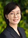
14:40 – 15:05 Invited Speech
Senior Expert for Quantum Sensors, Robert Bosch GmbH
Germany
Beyond the Hype: Quantum Sensors for Practical Applications
Abstract:
Sensor development is on the brink of a massive leap forward, thanks to quantum technologies. These aren’t just incremental improvements; quantum physics is pushing detection limits and accuracy to their absolute maximum. The “second quantum revolution” is moving these cutting-edge quantum concepts out of academic settings and into industry. Here, teams of physicists and engineers are taking large, laboratory-based quantum setups and shrinking them into robust, high-quality, and highly manufacturable quantum sensors. The key to making these innovative products a reality for everyday use – like magnetometers that could revolutionize cardiac care or sensors for navigation without GPS – lies in making them affordable, compact, lightweight, and power-efficient.
CV:
Tino Fuchs studied physics at the Humboldt University of Berlin and earned his doctorate there with his research work at the Max Planck Institute for Plasma Physics, in the Plasma Diagnostics division, in the field of x-ray spectroscopy of highly charged ions. Immediately after completing his doctorate, he transitioned to industry at Robert Bosch GmbH. After moving from the Automotive Electronics business unit to Corporate Research he embarked on a career as project manager and technical expert in the field of Advanced Technologies and Micro Systems. Since 2017, he has been a senior expert for quantum sensors and leads the associated research activity.

16:30 – 17:10 Keynote Speech
Senior Managing Executive Officer, Head of Engineering Center, Rapidus Corporation
Japan
The Made-in-Japan Challenge: A Paradigm Shift Enabled by Chiplet Technology
メイド・イン・ジャパンの挑戦:チップレット技術が拓く新次元への道
Rapidus株式会社
専務執行役員 エンジニアリングセンター長
折井 靖光
Abstract:
The semiconductor industry has entered a new era in which performance improvements are demanded in both front-end and back-end processes.
In this talk, I will introduce the new value created through the integration of these processes, with a focus on Rapidus’s initiatives in next generation chiplet technologies. Specifically, I will discuss differentiation strategies in advanced packaging, including large-panel-based assembly approaches,fine-pitch interconnect technologies, frameworks for integrating design and manufacturing, and evaluation and analysis techniques for ensuring reliability.
These efforts go beyond technological innovation alone—We aim to enrich people’s lives and deliver new value to society through the power of semiconductors.
CV:
Dr. Yasumitsu Orii joined IBM Japan in 1986 and was a leading expert on Flip Chip organic packages, which had contributed to the performance improvements and miniaturization of such products as servers, laptop
computers, and HDDs. The packaging technology is becoming more important for next generation server products as Moore’s Law reaches its limits. His flip chip expertise extended into many related areas. Initially, he was a pioneer of flip chip on FPC (Flexible Printed Circuit) for HDDs, which allowed the read/write amplifier ICs to be mounted on the suspension and much closer to the GMR head. Later, he eveloped the C2 (Chip Connection) technology that supported low-cost 50-μm-pitch flip chip bonding for the commodity consumerelectronics market and it was licensed to a company in Taiwan. At IBM Research Tokyo, he was leading the next generation flip chip organic package, 3D-IC projects and Neuromorphic Computing for IBM Servers and creating new technologies under a Joint Development Program involving many leading Japanese materials companies. He left IBM in 2014 and joined NAGASE & CO., LTD. He established “New Value Creation Office” under the direct control of the president and launched the material informatics software as a service in 2020. He left NAGASE and he joined Rapidus Corporation in 2022/Dec. Now he is the senior managing executive officer to lead the Engineering Center.
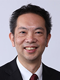
17:10 – 17:35 Invited Speech
Chief DTB Researcher/Development Dept., Tazmo co.,LTD
Japan
Advancements in Direct Transfer Bonding (DTB) for High-Precision Integration of Ultra-Thin and Delicate Chips
ダイレクト・トランスファー・ボンディング(DTB)の革新 —極薄・繊細チップの高精度集積に向けて—
タツモ株式会社
DTB首席研究員/開発部
佐野 一郎
Abstract:
Direct Transfer Bonding (DTB) technology has been developed to address the growing demand for high-precision die-to-wafer bonding in 3DIC and heterogeneous integration. Unlike conventional pick-and-place methods, DTB utilizes a surface-non-contact approach where chips are transferred directly from a carrier tape to a target wafer. This unique process minimizes contamination risks and enables exceptional alignment accuracy of less than 50 nm. A critical component for successful DTB is the specialized carrier tape, which must possess high infrared transparency for alignment and optimized adhesive properties. This presentation highlights recent advancements in DTB, specifically focusing on the integration of ultra-thin chips. By developing a new low-adhesion carrier tape designed for delicate handling, we successfully demonstrated the bonding of 10-µm-thick SiO2 chips with a high success ratio of 97%. These results indicate that the optimization of “peripheral peeling” during the transfer process is key to overcoming the challenges of handling extremely thin and flexible dies. DTB provides a simple, cost-effective, and highly accurate solution for the next generation of advanced packaging.
CV:
Ichiro Sano earned his master’s degree from Yamanashi University in 1993. With over three decades of leadership in semiconductor manufacturing technology, he has consistently spearheaded high-impact projects. In 2001, he led the development of a 300mm wafer batch cleaning system, establishing a fundamental expertise in wafer processing.
Since 2017, Ichiro has focused his expertise on Hybrid Bonding technology. Currently, as a Chief Researcher at TAZMO Co., Ltd., he plays a pivotal role in leading the development of Direct Transfer Bonding (DTB) for advanced Chip-on-Wafer (CoW) applications. Seeking to bridge industrial innovation with academic excellence, he enrolled in a doctoral program at Tohoku University in 2025. He is dedicated to advancing next generation 3DIC integration through his dual role in industry and academia.

Wednesday, April 22, 2026
8:35 – 9:15 Keynote Speech
CTO, Silex Microsystems AB
Sweden
The Next Decade of MEMS Manufacturing and Technology– A View from The World’s Largest Pure-Play MEMS Foundry
Abstract:
This keynote from Silex Microsystems presents a forward-looking perspective on MEMS and sensor manufacturing over the next decade. As demand continues to grow in established markets such as automotive, consumer electronics, and healthcare, MEMS foundries must evolve to deliver more advanced process technologies while scaling to higher production volumes. Examples will illustrate how foundries must adapt their capabilities to support increasing performance, reliability, and integration requirements. Beyond traditional markets, the most transformative growth lies in emerging applications including telecom, AR/VR, quantum technologies, photonics, and especially artificial intelligence. AI is rapidly moving beyond the data center into the physical world, giving rise to Physical AI—the integration of advanced sensing, edge computing, and micro-actuation that enables systems to perceive, decide, and act in real time. Just like our senses provide data to our brains, MEMS are now the Synthetic Senses that perceive the world for digital AI. As the physical interface between algorithms and reality, MEMS technologies are foundational to this shift. For MEMS foundries, this represents more than market expansion—it marks a structural transition toward enabling the intelligent, autonomous systems that will define the next generation of industry and infrastructure.
CV:
Dr. Niklas Svedin serves as Chief Technology Officer of Silex Microsystems AB, Sweden. He received his M.Sc. degree in Electrical Engineering in 1995 and his Ph.D. in MEMS in 2003, both from the Royal Institute of Technology (KTH) in Stockholm, Sweden. Dr. Svedin is one of the co-founders of Silex Microsystems and has been with the company since its establishment in 2000. Throughout his tenure, he has led numerous key customer programs and contributed significantly to the company’s technical and organizational development. In 2006, he was appointed Director of Engineering, assuming responsibility for technical review processes and support of new foundry platforms and products. In his current role as CTO, Dr. Svedin oversees the company’s strategic technology development and long-term innovation roadmap. He has made substantial contributions to the advancement of several core process technologies that form the foundation of Silex’s value proposition, including Sil-Via®, Met-Via®, low-temperature eutectic bonding, and temporary carrier bonding technologies.

9:15 – 9:40 Invited Speech
Director Business & Strategy, X-FAB MEMS Foundry
Germany
Advancements in Silicon Photonics and MEMS Through Heterogeneous Integration
Abstract:
Heterogeneous integration (HI) is emerging as a key enabler for next generation silicon photonics, leveraging manufacturing principles long established in MEMS to combine diverse material systems on a single platform. Building on methods such as wafer bonding, thin film processing, high precision lithography, and through wafer interconnects—techniques familiar to MEMS engineers—HI enables the integration of III V optoelectronic devices, advanced modulators, and functional sensing layers with silicon and silicon nitride photonic circuits. These approaches support compact, high performance solutions for applications spanning high speed communications, quantum technologies, medical sensing, and imaging. Recent progress in micro transfer printing and die to wafer assembly extends MEMS microfabrication principles to photonic chiplets, improving source-material efficiency and enabling scalable, manufacturable architectures. The convergence of photonics and MEMS-compatible integration technologies is driving new “more than photonics” systems that combine photonic, electrical, and microfluidic elements within a unified process flow. This presentation outlines key HI methodologies and trends and highlights how MEMS-derived manufacturing capabilities are shaping the future of heterogeneous photonic system integration.
CV:
Stefan Ernst studied physics at in Dresden, Germany and Edinburgh, UK. He received a PhD for research on magnetic quantum matter at the Max Planck Instititute in Dresden and at the University of Madrid. At X-FAB Semiconductor Foundries, Stefan held several positions in technology development, program management and marketing, covering high-voltage CMOS, wide-bandgap and sensor technologies. In his current role as Director Business & Strategy, he overlooks business development for MEMS, Microsystems and Photonics at the X-FAB Group, a leading European Semiconductor Foundry in the Analo/Mixed-Signal Space.

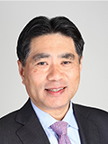
9:40 – 10:05 Invited Speech
Representative Director, Syntiant Japan KK
Japan
Syntiant: Making Edge AI a reality with MEMS Sensors
Syntiant: MEMSセンサーとEdge AIの融合
Syntiant Japan株式会社
代表取締役
鈴木 寛
Abstract:
Syntiant Corp. establishes itself as a leader in delivering hardware and software solutions for edge AI deployment. The presentation highlights significant advancements in MEMS microphones and vibration sensors, paired with ultra-low-power deep neural network processors. These innovations drive efficient “always-on” voice, audio, and vision applications across automotive, consumer electronics, and industrial sectors. A defining milestone in this evolution is the fusion of MEMS sensors with Edge AI capabilities, following Syntiant’s strategic acquisition of Knowles Corporation’s Consumer MEMS Microphone division. This integration positions the company at the forefront of AI-driven sensor solutions, enabling smarter devices that process data locally with high performance and minimal power consumption.
CV:
Hiroshi Suzuki is the Representative Director of Syntiant Japan, where he is responsible for MEMS sensors and AI solutions for the Japanese market. He joined Syntiant in December 2024 following the company’s acquisition of the Knowles Consumer MEMS Microphone division, where he had served as Representative Director of the Japan entity since 2019.
Prior to Knowles, he served as Country Manager and Vice President at Synaptics. His previous roles also include President of Motorola Mobility Japan, as well as various management positions at Ericsson, Nortel Networks, and IBM. He holds a Master’s degree in Nuclear Engineering from Nagoya University (1985).
10:05 – 10:30 Invited Speech
Founder/CTO, Frore Systems
USA
AirJetTM – A Novel Heat Dissipation Device
Abstract:
As consumer electronics and embedded systems demand increasingly higher processing power within shrinking form factors, thermal management has become a primary bottleneck for performance. Frore Systems addresses this critical challenge through the introduction of AirJet®, the world’s first solid-state active cooling chip. Unlike traditional mechanical fans, which are limited by size, noise, and mechanical failure points, Frore’s technology utilizes ultrasonic vibrating membranes to generate high-velocity pulsating jets. This mechanism creates significant back pressure enabling efficient heat dissipation through dust-proof, millimeter-thin vents. This abstract explores how Frore Systems’ solid-state approach allows devices—ranging from laptops, SSDs and IoT modules—to sustain significantly higher work loads without thermal throttling. By decoupling cooling capacity from device thickness, Frore Systems effectively signals a paradigm shift in thermal engineering, offering a silent, scalable solution that doubles performance in compact electronic architectures.
CV:
Dr. Suryaprakash (Surya) Ganti is the Co-Founder and Chief Technology Officer of Frore Systems and a pioneer in advanced thermal management. He is the primary architect behind AirJet®, the world’s first solid-state active cooling chip designed to replace traditional mechanical fans in consumer electronics. Surya has held many leadership roles at Qualcomm. As VP and head of R&D for Qualcomm MEMS Technology, he led the development of three generations of MEMS displays. Most recently, he drove R&D, development & operations of Ultrasonic Fingerprint technology for Qualcomm from Inception to High Volume Production with several successful product launches. Surya holds over 100 patents, has a bachelor’s degree from Indian Institute of Technology Madras, and a Ph.D. in Mechanical Engineering from the Massachusetts Institute of Technology.

11:45 – 12:35 Panel Discussion
Learning from failure in MEMS
NTHU Chair Professor, Power Mech. Eng. Department, National Tsing Hua University
Taiwan

Silicon Valley Band of Angels
USA
CV:
Kurt Petersen received his BS degree cum laude in EE from UC Berkeley in 1970, and a PhD in EE from the Massachusetts Institute of Technology in 1975. Since 1982, he has co-founded six successful, high-tech companies in Silicon Valley, including NovaSensor (now owned by Amphenol), Cepheid (acquired by Danaher in 2016 for $4B), and SiTime (SITM on NASDAQ). In 2001, he was awarded the IEEE Simon Ramo Medal for his contributions to MEMS. Dr. Petersen is a member of the National Academy of Engineering and is a Life Fellow of the IEEE in recognition of his contributions to “the commercialization of MEMS technology”. In 2011, Dr. Petersen joined the Silicon Valley Band of Angels. Today, he spends most of his time helping and mentoring early stage, high-tech start-up companies. In 2019, Dr. Petersen was awarded the IEEE Medal of Honor, IEEE’s highest tribute.

MEMS Industrial Partnerships Manager, CEA LETI
France

Founder/CTO, Frore Systems
USA

Sumitomo Precision Products/Chair of MEF Program WG
Japan
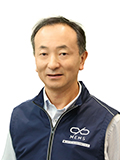
14:05 – 14:30 Invited Speech
Vice President, MEMS Engineering, SiTime Corporation
USA
SiTime MEMS: Vision and Persistence that Redefined Timing
Abstract:
In 20 years leading SiTime’s MEMS team, I have learned the value of setting a high bar for the performance of our future products, and then relentlessly pursuing those goals. SiTime’s very early products were not market-differentiated. We focused on development of our first-generation technology and learning about the market. This led to stagnant revenue. Each year we made improvements, and in 2008, my team laid out the first steps of our MEMS technology vision. Combined with advancements in circuits and packaging, it began to pay off in 2013 with our first differentiated products that excelled in power, small size, precision, and robustness. Subsequently, SiTime invested years of effort to solve our customers’ most difficult timing challenges. The practice of setting ambitious goals, even when not knowing how to reach them, and then relentlessly driving toward them, has paid off. We achieved every goal and developed new categories of timing products along the way. SiTime now leads the industry in precision timing, servicing thousands of applications including oscillators for high-bandwidth data networks and ppb-level stability, with over 4 billion units shipped.
CV:
Paul is passionate about entrepreneurship and innovation. He joined SiTime in 2005 to direct the development of microelectromechanical systems (MEMS) resonators. Paul’s team delivered the industry’s first volume production MEMS resonators for timing. His team launched 6 generations of MEMS resonator technologies, supporting timing products that lead the industry in performance, size, and reliability, with 4 billion devices shipped. Prior to joining SiTime, Paul co-founded C Speed Corporation in 1998, where he led the development of MEMS micromirrors for optical switching. He holds a Bachelor of Science degree in Engineering from Harvey Mudd College, a Master’s of Science degree in Mechatronics and Optical Engineering from Loughborough University, and a Ph.D. in Electrical Engineering from U.C. Davis. Paul holds over 70 patents in the fields of MEMS and optical systems.

14:30 – 14:55 Invited Speech
CTO, Resonant Inc., a Murata Company
USA
XBAR Technology for RF Filter Applications
Abstract:
Murata has recently launched mass production and commercial shipment of a new type of high-frequency acoustic resonator for RF filtering called XBAR. These MEMS devices use a laterally eXcited shear-wave Bulk Acoustic Resonance (XBAR) mode, engineered to provide the high acoustic coupling (bandwidth) that improves wideband filters required for 5G, WiFi, and 6G radio applications above 3 GHz. In this talk, we will describe how the XBAR structure enabled SAW-like devices to extend up to the 10 GHz range while maintaining the excellent performance metrics required for low-loss/high-rejection filters. We will also review some related technologies and explain the role of simulation-led rapid technology development cycles that married with manufacturing excellence to launch the first new class of acoustic resonator for RF filters in the past twenty years.
CV:
Dr. Patrick J. Turner received the B.Sc. degree in physics from McMaster University, Hamilton, ON, Canada, in 1997 and the M.Sc. and Ph.D. degrees in physics from the University of British Columbia, Vancouver, BC, Canada, in 1999 and 2005, respectively. His PhD research was in low temperature RF studies of unconventional superconductivity with Dr. Walter Hardy. In 2007 he joined Superconductor Technologies Inc, Santa Barbara CA, USA, and then Resonant Inc., San Mateo CA, USA in 2012 where he has focused on acoustic wave resonators for RF filter applications. Resonant was acquired by Murata in 2022. Currently, Dr. Turner is the CTO of Resonant Inc. and is responsible for new technology and IP development. He is named on over 100 technical articles and U.S. Patents.

14:55 – 15:20 Invited Speech
Yokogawa Products Headquarter Sensing Center, Yokogawa Electric Corporation
Japan
Silicon Resonant Sensor Technology: Applications in Tsunami Disaster Mitigation
シリコンレゾナントセンサ技術と津波防災への応用
横河電機株式会社
横河プロダクト本部センシングセンター
𠮷田 周平
Abstract:
We will introduce our silicon resonant sensor and its role in tsunami disaster mitigation.
This sensor offers outstanding long-term stability thanks to its unique measurement principle, making it highly competitive in the market for pressure transmitters and digital manometers, where reliability and measurement stability are essential.
Recently, we developed a water pressure gauge based on an upgraded silicon resonant sensor, which has been deployed in the Nankai Trough Seafloor Observation Network for Earthquakes and Tsunamis (N-net). N-net is part of Japan’s nationwide observation network for earthquakes, tsunamis, and volcanoes over land and sea. In this talk, we will share the background and the deployment achievements.
CV:
Yokogawa Electric Corporation is a global company with a long history in industrial automation and measurement.
In the field of MEMS, the company has been engaged in the development of silicon resonant MEMS–based pressure sensors for industrial applications, covering device design, process development, and technical studies toward volume production. Emphasis is placed on long-term stability and reliability required for industrial use, with development efforts directed toward practical MEMS sensors suitable for field operation.
Shuuhei Yoshita is an engineer at Yokogawa Electric Corporation with more than 15 years of experience in MEMS process technology. He has been involved in the development of silicon resonant pressure sensors, focusing mainly on MEMS process development and process integration. His work spans research and development activities as well as technical considerations toward manufacturable and reliable MEMS devices for industrial applications.

15:20 – 15:45 Invited Speech
Professor, Kyoto University/CTO, Physios Biotech, Inc.,
Japan
京都大学/株式会社フィジオスバイオテック
教授/取締役
横川 隆司
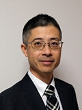
CEO, Physios Biotech, Inc.Japan
株式会社フィジオスバイオテック
代表取締役
三木 一郎

Drug Discovery Innovation and Social Implementation Enabled by Microphysiological Systems (MPS): Opportunities from Japan
Abstract:
Microphysiological Systems (MPS), which reconstruct human physiological microenvironments using microfluidic devices, are increasingly recognized as a core technology within Non-Animal Methods (NAMs). While artificial intelligence and organoids can be readily integrated into existing drug discovery pipelines, MPS require careful alignment with specific phases of development and clearly defined use cases, posing unique challenges for social and industrial implementation.
In this talk, we present current efforts toward the social implementation of MPS in Japan from the perspective of microfabrication and MEMS-based engineering. Our work is centered on the development of perfusable on-chip vascular networks, which serve as a common technological platform for interfacing parenchymal cells and vascular endothelial cells. By leveraging both two-dimensional (2D-MPS) and three-dimensional (3D-MPS) architectures, we have established a range of assay systems that recapitulate key physiological functions of the kidney, respiratory system, brain, and tumor microenvironments.
Beyond applications in drug discovery and safety assessment, these MPS platforms are increasingly utilized for fundamental biological studies, including vascular biology and tissue maturation. Finally, we discuss the technical challenges, opportunities for industrial collaboration, and the evolving role of MEMS technologies in advancing MPS from laboratory research toward scalable and reliable social implementation.
CV:
Prof. Ryuji Yokokawa
Ryuji Yokokawa is a Professor at Department of Micro Engineering, Kyoto University, Japan, CTO at Physios Biotech Inc, and a Visiting Researcher at RIKEN Center for Biosystems Dynamics Research (BDR), Japan. He received his Ph.D. from the Department of Electrical Engineering at The University of Tokyo. He earned his B.S. and M.S. degrees in Mechanical Engineering from Kyoto University. He has authored or co-authored over 100 peer-reviewed journal papers and 200 conference papers. He has received 38 academic awards. He is a member of ISSCR, IMPSS, IEEE, BMES and other international societies.
Dr. Ichiro Miki
On July 1, 2025, he assumed the position of CEO at Physios Biotech Co., Ltd., where he oversees the company’s overall management and leverages his pharmaceutical industry experience to spearhead the practical application of MPS. Additionally, as the representative of Mityiro Research Institute, he supports industry-academia collaboration. Prior to joining Physios Biotech, he supported venture capital and startups through Drug Discovery Venture Ecosystem Program at AMED, managed research at a tech venture, and supported the social implementation of academia seeds Center of Innovation (COI) Program at JST. He also engaged in new drug discovery and development at Kyowa Hakko Kogyo for 25 years. He holds a Ph.D. from the University of Tokyo Faculty of Pharmaceutical Sciences and a Master degree from Kyoto University Faculty of Science.
16:15 – 16:40 Invited Speech
Chief Technology Officer (CTO), TactoTek
Finland
Smart Surfaces Through IMSE® Integration
(Initial Title (to be confirmed))
Abstract:
TactoTek® develops, productizes, and licenses IMSE® In-Mold Structural Electronics. IMSE is a breakthrough technology that enables integration of electronics directly into 3D-molded plastic structures. IMSE replaces traditional multi-part assemblies with a single integrated part. This leads to smaller construction space, lower weight and ultimately lower emissions. TactoTek has widely patented the IMSE technology and holds 50 patent families with more than 300 granted patents worldwide.
Automotive is one of the leading industries adopting IMSE technology. Automotive interiors are transforming from driver-centric vehicles into multimodal spaces. Surfaces will sense the environment and will interact with people. IMSE is an enabler of this transition – turning decorative surfaces into living, smart surfaces that communicate through light, sense and interaction. In this presentation, efficient electronics integration technology IMSE will be presented and application examples in automotive are being introduced. Also, first insights into how MEMS could be integrated into IMSE will be shared.
CV:
Dr. Pälvi Apilo is the Chief Technology Officer at TactoTek. As CTO, she drives the company’s long-term technology vision, leading innovation, emerging technologies, and the strategic development of TactoTek’s globally recognized intellectual property portfolio. With over 20 years of experience in applied research, technology foresight, EU and national funding, and international cross-disciplinary collaboration, she bridges scientific insight with business strategy to advance sustainable and scalable electronics. Before her appointment as CTO, Pälvi served as Director of Foresight and Research at TactoTek, where she led initiatives that strengthened the company’s technology leadership and expanded its capabilities in automotive and circular electronics. Earlier in her career, she worked for more than a decade at VTT Technical Research Centre of Finland, responsible for planning, executing, and delivering both demanding EU- and nationally funded projects as well as customer projects on printed and hybrid electronics, and worked as a visiting researcher at Fraunhofer ISE in Germany. Pälvi holds an M.Sc. in Electronics and Electrical Engineering from the Helsinki University of Technology and a Ph.D. in Printed Electronics from the University of Oulu.

16:40 – 17:05 Invited Speech
Chief Specialist, Micro Electronics Development Group, Mask Lithography Development Department , NuFlare Technology
Japan
MBM™ series: MEMS-Enabled Electron Multi-Beam Mask Writer for EUV Lithography
MBM™シリーズ:MEMS技術により実現されたEUV向けマルチ電子ビームマスク描画装置
株式会社ニューフレアテクノロジー
描画装置開発部 マイクロエレクトロニクス開発グループ参事
東 和幸
Abstract:
This talk will cover the latest progress on the advanced photomask writing system MBM-4000, focusing on improvements in writing performance and the essential role of MEMS technology in achieving these innovations.
CV:
Expert in semiconductor process technology with over 20 years of experience at Toshiba, driving the development of advanced logic and memory products. Currently focused on 3D integration and MEMS device innovation to enable next-generation semiconductor solutions.
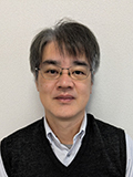
17:05 – 17:30 Invited Speech
Director Engineering, Lam Research
The Netherlands
Advances in thin films enabled by Lam Research’ Pulsed Laser Deposition platform for MEMS applications
Abstract:
Pulsed laser deposition (PLD) is a very versatile thin film deposition technology that has the ability to deposit a wide range of advanced thin film materials. With today’s market demand for enhanced and new material systems, PLD enables layers that cannot practically be deposited by conventional technologies like reactive sputtering (PVD). This deposition solution enables more advanced device design and is driving the next generation of radio frequency (RF) filters for 5G, WiFi 6 and 6E, high-end micro-electromechanical systems (MEMS), ferroelectric memory and photonics applications.
For piezoelectric aluminum scandium nitride, PLD has extended the limits of scandium doping in the AlScN compound, resulting in very high piezoelectric properties. Additionally, this PLD platform enables precise control over thickness, uniformity and thin film stress, which are crucial for high-yield (RF) MEMS applications.
For the first time in semiconductor production, Lam is using lasers to deposit thin films and brings PLD to wafer-level mass production. Lam Research PLD is expected to be key in developing cutting-edge specialty technologies devices, such as RF filters for 5G and Wi-Fi 6 and high-end MEMS microphones.
CV:
Matthijn Dekkers received his PhD in Applied Physics at University of Twente in 2007. In the same year he co-founded the company SolMateS. As CTO he ran the R&D division that scaled the Pulsed Laser Deposition technique (PLD). In 2022 SolMateS was acquired by Lam Research, and he became Director Engineering PLD.

17:30 – 17:55 Invited Speech
Product marketing Manager, Evatec AG
Switzerland
Enabling the Future of RF Filters: High-Performance Thin Films for BAW Technology
Abstract:
As the wireless industry moves toward 6G, advanced RF filter technologies with improved high-frequency performance and manufacturability are required. This presentation reports recent progress in high-volume sputtering processes for RF filter thin films using Evatec’s CLUSTERLINE® 200 platform. High-Sc AlScN films, low-resistivity Mo electrodes, and in-situ c-axis polarity control without vacuum break are demonstrated. These results confirm the industrial readiness of scalable, high-performance AlScN-based RF filter manufacturing.
CV:
2005-2010 BSc: Physics Engineering at Ankara University, Advanced magnetic force microsopy on nanostructured NdFeB ribbons
2010-2012 MSc: Physics at Ankara University on magnetocaloric effect of semi-Heusler alloys
2012-2016 PhD: Physics at Helmholtz Zentrum Dresden Rossendorf and TU Dresden on Effect of microstructure on the magnetic properties of transition metal implanted TiO2 films
2016-2017 PostDoc at Helmholtz Zentrum Dresden Rossendorf on ion irradiation modification of antiferromagnetic thin films for high frequency communication
2017-2020 Post Doc at EMPA Zurich on development of an off-axis sputtering cathode for epitaxial growth of sub-nm thin films
2020-2022 Scientific Group leader at EMPA Zurich. Focusing on thin film applications on logic and biomedical applications
2022-2023: Process development engineer at Evatec AG on development of high Sc content AlScN and highly conductive Mo layers
2024-…: Product Marketing Manager at Evatec AG responsible for wireless communication solutions
<40 papers and patent applications
